
Digital Light Processingtm for High-Brightness, High-Resolution Applications
Larry J. Hornbeck
hbek@dlep1.itg.ti.com
Texas Instruments
Digital Video Operations
Dallas, Texas 75265
Electronic projection display technology for high-brightness applications had its origins in the Gretag Eidophor, an oil film-based projection system developed in the early 1940s. A number of solid state technologies have challenged the Eidophor, including CRT-addressed LCD light valves and active-matrix-addressed LCD panels. More recently, in response to various limitations of the LCD technologies,high-brightness systems have been developed based on Digital light Processing tm technology. At the heart of the DLP tm projection display is the Digital Micromirror Device tm (DMD)tm, a semiconductor-based array of fast, reflective digital light switches that precisely control a light source using a binary pulse width modulation technique.
This paper describes the design, operation, performance, and advantages of DLP-based projection systems for high-brightness,high-resolution applications. It also presents the current status of high-brightness products that will soon be on the market.
Key Words: Digital Micromirror Device, DMD, Digital Light Processing, DLP, spatial light modulator, SLM,micro-electromechanical systems, MEMS, digital imaging,projection displays.
INTRODUCTION
Large-screen, high-brightness electronic projection displays serve four broad areas of application: (1) Electronic presentations (e.g., business, education, advertising), (2) entertainment (e.g., home theater, sports bars, theme parks,electronic cinema), (3) status and information (e.g., military,utilities, transportation, public, sports) and (4) simulation (e.g.,training, games). The electronic presentation market is being driven by the pervasiveness of software that has put sophisticated presentation techniques (including multimedia) into the hands of the average PC user.
A survey of
high-brightness (>1000 lumens) electronic projection displays
is shown in Figure 1. 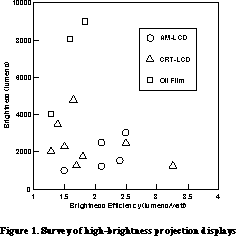 The brightness (lumens) is plotted against the brightness efficiency (lumens/watt).Three
types of projection display technologies are compared in Figure 1, oil film,
CRT-LCD, and AM-LCD. Developed in the early 1940s at the Swiss Federal Institute
of Technology and later at Gretag AG, oil film projectors (including the GETalaria)
have been the workhorse for applications that require projection displays of
the highest brightness [1]. But the oil film projector has a number of limitations
including size,weight, power, setup time, stability, and maintenance. In response
to these limitations, LCD-based technologies have challenged the oil film projector.
These LCD-based projectors are of two general types: (1) CRT-addressed LCD lightvalves
and (2) active-matrix (AM) LCD panels.
The brightness (lumens) is plotted against the brightness efficiency (lumens/watt).Three
types of projection display technologies are compared in Figure 1, oil film,
CRT-LCD, and AM-LCD. Developed in the early 1940s at the Swiss Federal Institute
of Technology and later at Gretag AG, oil film projectors (including the GETalaria)
have been the workhorse for applications that require projection displays of
the highest brightness [1]. But the oil film projector has a number of limitations
including size,weight, power, setup time, stability, and maintenance. In response
to these limitations, LCD-based technologies have challenged the oil film projector.
These LCD-based projectors are of two general types: (1) CRT-addressed LCD lightvalves
and (2) active-matrix (AM) LCD panels.
LCD-based projectors have not provided the perfect solution for the entire range of high-brightness applications. CRT-addressed LCD light valves have setup time and stability limitations. Most active-matrix LCDs used for high-brightness applications are transmissive and, because of this, heat generated by light absorption cannot be dissipated with a heat sink attached to the substrate. This limitation is mitigated by the use of large-area LCD panels with forced-air cooling. However, it may still be difficult to implement effective cooling at the highest brightness levels.
In response to these and other limitations, 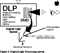 as well as to provide superior image quality under the most demanding environmental
conditions, high-brightness projection display systems have been developed based
on Digital Light Processing tm technology. DLP tm is based
on a micro-electromechanical system (MEMS) device known as the Digital Micromirror
Device tm (DMD)tm. The DMD, invented in 1987 at Texas
Instruments, is a semiconductor-based array of fast, reflective digital light
switches that precisely control a light source using a binary pulse width modulation
technique. It can be combined with image processing, memory, a light source,
and optics to form a DLP system (Figure 2) capable of projecting large,
bright, seamless, high-contrast color images.
as well as to provide superior image quality under the most demanding environmental
conditions, high-brightness projection display systems have been developed based
on Digital Light Processing tm technology. DLP tm is based
on a micro-electromechanical system (MEMS) device known as the Digital Micromirror
Device tm (DMD)tm. The DMD, invented in 1987 at Texas
Instruments, is a semiconductor-based array of fast, reflective digital light
switches that precisely control a light source using a binary pulse width modulation
technique. It can be combined with image processing, memory, a light source,
and optics to form a DLP system (Figure 2) capable of projecting large,
bright, seamless, high-contrast color images.
Figure 3 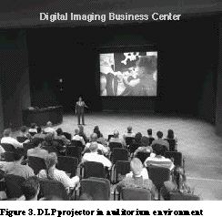 shows
a DLP projector in an auditorium environment. This photo was taken at the Texas
instruments Digital Imaging Business Center in Dallas, Texas.
shows
a DLP projector in an auditorium environment. This photo was taken at the Texas
instruments Digital Imaging Business Center in Dallas, Texas.
DLP-based projection displays are well-suited to high-brightness and high-resolution applications: (a) the digital light switch is reflective and has a high fill factor, resulting in high optical efficiency at the pixel level and low pixelation effects in the projected image; (b) as the resolution and size of the DMD increase, the overall system optical efficiency grows because of higher lamp-coupling efficiency; (c) because the DMD operates with conventional CMOS voltage levels (~5volts), integrated row and column drivers are readily employed to minimize the complexity and cost impact of scaling to higher resolutions; (d) because the DMD is a reflective technology,the DMD chip can be effectively cooled through the chip substrate, thus facilitating the use of high-power projection lamps without thermal degradation of the DMD; and(e) finally, DLP-based systems are all-digital (digital video in, digital light out), so reproduction of the original video source material is accurate and the image quality is stable with time [2].
The general movement of the display industry is in the digital direction. Digital sources that are currently available include digital video disk (DVD), digital satellite system(DSS), and the Internet (World Wide Web). In the future, the recently approved Advanced Television Standard (ATV) and the digital distribution of movies (digital cinema) will be added to the list of digital sources. Interfacing these digital sources to currently available analog displays requires digital-to-analog conversion and, in some instances, analog encoding (e.g., s-video or composite), which result in degradation of the source image quality. DLP-based displays, on the other hand, preserve the digital integrity of the source image all the way to the eye. The result is the best possible video quality.
A comprehensive, chronological list of DLP and DMD publications and presentations [2-59] is presented in Section 8.0.The list includes general DLP review papers and papers on early DMD development, system electronics, optics, DMD mechanical modeling, manufacturing, and reliability. It also includes references to DMD-based digital printing technology [4,24,37,56].
DMD LIGHT SWITCH
2.1 The mirror as a switch
The DMD light switch (Figure 4) is a member of a class of devices known
as micro-electromechanical systems.
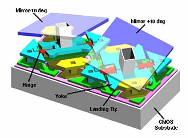
Other MEMS devices include pressure sensors, accelerometers, and microactuators. The DMD is monolithically fabricated by CMOS-like processes over a CMOS memory. Each light switch has an aluminum mirror, 16 um square, that can reflect light in one of two directions, depending on the state of the underlying memory cell. Rotation of the mirror is accomplished through electrostatic attraction produced by voltage differences developed between the mirror and the underlying memory cell. With the memory cell in the on (1) state, the mirror rotates to +10 degrees.
With the memory cell in the off (0) state, the mirror rotates to -10 degrees.
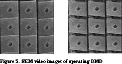
A close-up of DMD mirrors operating in a scanning electron microscope (SEM)
is shown in Figure 5.
2.2 Grayscale and color operation
Grayscale is achieved by binary pulse width modulation of the incident light. Color is achieved by using color filters, either stationary or rotating, in combination with one, two, or three DMD chips (Section 3.2).
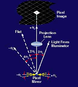
The DMD light switch is able to turn light on and off rapidly by the beam-steering action of the mirror. As the mirror rotates,it either reflects light into or out of the pupil of the projection lens, to create a burst of digital light pulses that the eye interprets as an analog image (Figure 2). The optical switching time for the DMD light switch is ~2 us. The mechanical switching time, including the time for the mirror to settle and latch, is ~15 us [36].
The technique for producing the sensation of grayscale to the observer's eye is called binary pulse width modulation. The DMD accepts electrical words representing gray levels of brightness at its input and outputs optical words, which are interpreted by the eye of the observer as analog brightness levels. The details of the binary pulsewidth modulation (PWM) technique are illustrated in Figure 7.
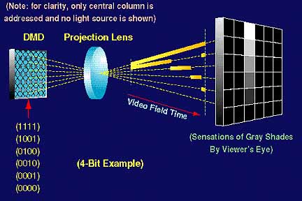
For simplicity, the PWM technique is illustrated for a 4-bit word (2 4 or 16 gray levels). Each bit in the word represents a time duration for light to be on or off (1 or 0). The time durations have relative values of 20,21, 22, 23, or 1, 2, 4, 8. The shortest interval (1) is called the least significant bit (LSB). The longest interval (8) is called the most significant bit (MSB). The video field time is divided into four time durations of 1/15, 2/15, 4/15, and 8/15 of the video field time. The possible gray levels produced by all combinations of bits in the 4-bit word are 24 or 16 equally spaced gray levels (0, 1/15, 2/15 . . . 15/15). Current DLP systems are either 24-bit color (8 bits or 256 gray levels per primary color) or 30-bit color (10 bits or 1024 gray levels per primary color). In the simple example shown in Figure 7, spatial and temporal artifacts can be produced because of imperfect integration of the pulsed light by the viewer's eye.
These artifacts can be reduced to negligible levels by "bit-splitting" technique [26]. In this technique, the longer duration bits are subdivided into shorter durations, and these split bits are distributed through-out the video field time. DLP displays combine pulsewidth modulation and bit-splitting to produce "true-analog" sensation, but with greater accuracy and stability than can be achieved by analog projection systems.
2.3 DMD cell architecture and fabrication
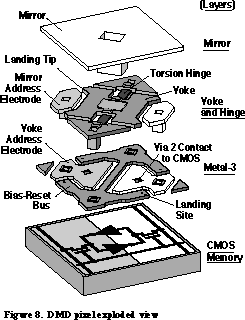
The DMD pixel is a monolithically integrated MEMS superstructure cell fabricated over a CMOS SRAM cell (figure 8) [51].
 An organic sacrificial layer is removed by plasma etching to produce air gaps
between the metal layers of the superstructure. The air gaps free the structure
to rotate about two compliant torsion hinges. The mirror is rigidly connected
to an underlying yoke. The yoke, in turn, is connected by two thin, mechanically
compliant torsion hinges to support posts that are attached to the underlying
substrate.
An organic sacrificial layer is removed by plasma etching to produce air gaps
between the metal layers of the superstructure. The air gaps free the structure
to rotate about two compliant torsion hinges. The mirror is rigidly connected
to an underlying yoke. The yoke, in turn, is connected by two thin, mechanically
compliant torsion hinges to support posts that are attached to the underlying
substrate.
The address electrodes for the mirror and yoke are connected to the complementary sides of the underlying SRAM cell.The yoke and mirror are connected to a bias bus fabricated at the metal-3 layer. The bias bus interconnects the yoke and mirrors of each pixel to a bond pad at the chip perimeter [36]. An off-chip driver supplies the bias waveform necessary for proper digital operation (Section 2.4). The DMD mirrors are 16 um square and made of aluminum for maximum reflectivity. They are arrayed on 17 um centers to form a matrix having a high fill factor (~90%). The high fill factor produces high efficiency for light use at the pixel level and a seamless (pixelation-free) projected image.
Electrostatic fields are developed between the mirror and its address electrode and the yoke and its address electrode, creating an efficient electrostatic torque. This torque works against the restoring torque of the hinges to produce mirror and yoke rotation in the positive or negative direction. The mirror and yoke rotate until the yoke comes to rest (or lands) against mechanical stops that are at the same potential as the yoke. Because geometry determines the rotation angle, as opposed to a balance of electrostatic torques employed in earlier analog devices, the rotation angle is precisely determined.
The fabrication of the DMD superstructure begins with a completed CMOS memory circuit. A thick oxide is deposited over metal-2 of the CMOS and then planarized using a chemical mechanical polish (CMP) technique. The CMP step provides a completely flat substrate for DMD superstructure fabrication, ensuring that the projector's brightness uniformity and contrast ratio are not degraded.
Through the use of six photomask layers, the superstructure is formed with layers of aluminum for the address electrode (metal-3), hinge, yoke and mirror layers and hardened photo-resist for the sacrificial layers (spacer-1 and spacer-2) that form the two air gaps. The aluminum is sputter-deposited and plasma-etched using plasma-deposited SiO2 as the etch mask. Later in the packaging flow, the sacrificial layers are plasma-ashed to form the air gaps.
The packaging flow begins with the wafers partially sawed along the chip scribe lines to a depth that will allow the chips to be easily broken apart later. The partially sawed and cleaned wafers then proceed to a plasma etcher that is used to selectively strip the organic sacrificial layers from under the DMD mirror, yoke, and hinges. Following this process, a thin lubrication layer is deposited to prevent the landing tips of the yoke from adhering to the landing pads during operation. Before separating the chips from one another, each chip is tested for full electrical and optical functionality by a high-speed automated wafer tester [55]. Finally, the chips are separated from the wafer, plasma-cleaned, relubricated, and hermetically sealed in a package. Further manufacturing details are contained in references [36, 43, 51, 52, 57].
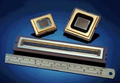
Figure 9 shows packaged DMD chips in two array sizes, SVGA (800 x 600) and SXGA (1280 x 1024). The diagonals of the active area, as discussed in Section 4.1, are 0.7 in.(SVGA) and 1.1 in. (SXGA).
2.4 Electronic operation
The DMD pixel is inherently digital because of the way it is electronically driven [5]. It is operated in an electrostatically bistable mode by the application of a bias voltage to the mirror to minimize the address voltage requirements. Thus, large rotation angles can be achieved with a conventional 5-volt CMOS address circuit.
The organization of the DMD chip is shown in Figure 10.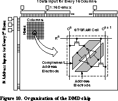 Underlying each DMD mirror and mechanical superstructure cell is a six-transistor
SRAM. Multiple data inputs and demultiplexers (1:16) are provided to match
the
frequency capability of the on-chip CMOS with the required video data rates.
The pulsewidth modulation scheme for the DMD requires that the video field
time
be divided into binary time intervals or bit times. During each bit time, while
the mirrors of the array are modulating light, the underlying memory array
is
refreshed or updated for the next bit time. Once the memory array has been
updated, all the mirrors in the array are released simultaneously and allowed
to move
to their new address states.
Underlying each DMD mirror and mechanical superstructure cell is a six-transistor
SRAM. Multiple data inputs and demultiplexers (1:16) are provided to match
the
frequency capability of the on-chip CMOS with the required video data rates.
The pulsewidth modulation scheme for the DMD requires that the video field
time
be divided into binary time intervals or bit times. During each bit time, while
the mirrors of the array are modulating light, the underlying memory array
is
refreshed or updated for the next bit time. Once the memory array has been
updated, all the mirrors in the array are released simultaneously and allowed
to move
to their new address states.
This simultaneous update of all mirrors, when coupled with the PWM bit-splitting algorithm described in Section 2.2, produces an inherently low-flicker display. Flicker is the visual artifact that can be produced in CRTs as a result of brightness decay with time of the phosphor.
Because CRTs are refreshed in an interlaced scan-line format, there is both a line-to-line temporal phase shift in brightness as well as an overall decay in brightness. DLP-based displays have inherently low flicker because all pixels are updated at the same time (there is no line-to-line temporal phase shift) and because the PWM bit-splitting algorithm produces short-duration light pulses that are uniformly distributed throughout the video field time (no temporal decay in brightness).
Proper operation
of the DMD is achieved by using the bias and address sequence shown in Figure
11 and detailed inTable 1.

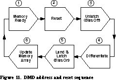
The bias voltage has three functions. First, it produces a bistable condition to minimize the address voltage requirement, as previously mentioned. In this manner, large rotation angles can be achieved with conventional 5-volt CMOS. Second,it electromechanically latches the mirrors so that they cannot respond to changes in the address voltage until the mirrors are reset. The third function of the bias is to reset the pixels so that they can reliably break free of surface adhesive forces and begin to rotate to their new address states.
Although the metal surfaces of the superstructure are coated with a passivation
layer or lubrication layer, the remaining van der Waal or surface forces between
molecules require more than the hinge-restoring force to reliably reset the
mirrors. A reset voltage pulse applied to the mirror and yoke causes the spring
tips of the yoke (Figure 12) to flex.
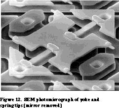
As the spring tips unflex, they produce a reaction force that causes the yoke landing tips to accelerate away from the landing pads,producing a reliable release from the surface [52].
2.5 DMD reliability
Steady improvements in DMD reliability have been made [28, 49, 52]. Some of these are listed below:
3.0 DLP SYSTEM DESCRIPTION AND OPERATION
3.1 System design [20, 27, 42].
Figure 13 illustrates a generic three-chip DLP system broken down into its functional components (video front-end, digital processor, digital formatter, and digital display). The generic video front-end accepts a variety of video sources (digital,digital compressed, digital graphics, analog composite, analogs-video, and analog graphics). The video front-end performs the functions of decompression, decoding, and analog-to-digital conversion, depending on the nature of the video source.
The first operation in the digital processor is progressive-scan conversion. This conversion is required if the original source material is interlaced. An interlaced format provides even lines of video during one video field time and odd lines during the next field time. Progressive-scan conversion is the process of creating (by an interpolation algorithm) new scan lines between the odd or even lines of each video field.
Interlacing has been historically used in CRT-based systems to reduce the video bandwidth requirements without producing objectionable flicker effects created by the temporal decay in phosphor brightness. For progressively scanned CRTs, interlacing is unnecessary because additional bandwidth is allocated so that every line of the CRT is refreshed during each field time. Progressive scanning that incorporates motion-adaptive algorithms helps to reduce interlace scanning artifacts such as interline flicker, raster line visibility, and field flicker. These are particularly noticeable in larger display formats.
The next operation in the digital processor is digital resampling (or scaling). This operation resizes the video data to fit the DMD's pixel array, expands letterbox video sources, and maintains a correct aspect ratio for the square pixel DMD format. After the scaling operation, the video data is input to the color space conversion block. If the video is not already in a red, green, blue (R,G,B) format, it is converted from luminance and color difference encoding (e.g., Y, CR , CB ) into R,G,B. Next, a degamma (inverse gamma) function is performed because, unlike CRTs, DMDs are linear displays. The degamma operation can produce low-light-level contouring effects, but these are minimized by using an error diffusion technique.
Finally the R,G,B signal is input to the digital formatter. First,the scan-line format data is converted into an R,G,B bit-plane format. The bit planes are stored in a dual-synchronous DRAM (SDRAM) frame buffer for fast access of the bit-plane data.The bit-plane data is then output to the DMDs in a PWM bit-splitting sequence (Section 2.2). As explained in Section 2.4,the DMD chip has multiple data inputs that allow it to match the frequency capability of the on-chip CMOS with the required video data rates. The bit-plane data coming out of the frame buffer is multiplexed 16:1 and fed to the multiple data inputs of each DMD. The bit-plane data is then demultiplexed 1:16 and fed to the frame-memory underlying the DMD pixel array.
3.2 Projection optics [44]
DLP optical systems have been designed in a variety of configurations distinguished
by the number of DMD chips (one,two, or three) in the system [44]. The one-chip
and two-chip systems rely on a rotating color disk to time-multiplex the colors.
The one-chip configuration is used for lower brightness applications and is the most compact. Two-chip systems yield higher brightness performance but are primarily intended to compensate for the color deficiencies resulting from spectrally imbalanced lamps (e.g., the red deficiency in many metalhalide lamps). For the highest brightness applications, three-chip systems are required.
A DLP optical system with three chips is shown in Figure 14. Because the DMD is a simple array of reflective light switches, no polarizers
are required. Light from a metal halide or xenon lamp is collected by a condenser
lens. For proper operation of the DMD light switch, this light must be directed
at 20 degrees relative to the normal of the DMD chip (Figure 6).To accomplish
this in a method that eliminates mechanical interference between the illuminating
and projecting optics, a total internal reflection (TIR) prism is interposed
between the projection lens and the DMD color-splitting/-combining prisms.
Because the DMD is a simple array of reflective light switches, no polarizers
are required. Light from a metal halide or xenon lamp is collected by a condenser
lens. For proper operation of the DMD light switch, this light must be directed
at 20 degrees relative to the normal of the DMD chip (Figure 6).To accomplish
this in a method that eliminates mechanical interference between the illuminating
and projecting optics, a total internal reflection (TIR) prism is interposed
between the projection lens and the DMD color-splitting/-combining prisms.
The color-splitting/-combining prisms use dichroic interference filters deposited on their surfaces to split the light by reflection and transmission into red, green, and blue components.The red and blue prisms require an additional reflection from a TIR surface of the prism in order to direct the light at the correct angle to the red and blue DMDs. Light reflected from the on-state mirrors of the three DMDs is directed back through the prisms and the color components are recombined.The combined light then passes through the TIR prism and into the projection lens because its angle has been reduced below the critical angle for total internal reflection in the prism air gap.
A DLP three-chip prototype projection engine is shown inFigure 15.
 It
projects 1100 lumens with a 500-watt xenon lamp. The size of the engine is 19.5
x 12.8 x 10 in. and it weighs 38 pounds. One of the DMD package assemblies with
thermoelectric cooler and fan is visible.
It
projects 1100 lumens with a 500-watt xenon lamp. The size of the engine is 19.5
x 12.8 x 10 in. and it weighs 38 pounds. One of the DMD package assemblies with
thermoelectric cooler and fan is visible.
4.0 DISPLAY PERFORMANCE
4.1 Resolution
DLP projection systems have been demonstrated at a variety of resolutions (and aspect ratios), VGA (640 x 480), SVGA (800 x 600) and SXGA (1280 x 1024). A 16:9 aspect ratio high-definition (1920 x 1080) DLP projection system has also been demonstrated [20, 27, 35]. Currently there are DLP-based products on the market for business applications at SVGA resolution. Both professional (high-brightness) and business products will be available at XGA resolution by the end of 1997. SXGA products will follow in 1998.
The DMD family of chips uses a common pixel design having a 16 um mirror arrayed with a 17 um pixel pitch. As the DMD resolution is increased, the pixel pitch is held constant and the chip diagonal is allowed to increase. This approach to the chip design has several advantages: (1) the high optical efficiency and contrast ratio of the pixel is maintained at all resolutions, (2) pixel timing is common to all designs and high address margins are maintained, and (3) the chip diagonal increases with resolution, which improves the DMD system optical efficiency (see Section 4.2).
4.2 Optical efficiency and brightness.
The optical efficiency of the DLP projection system is the product of the efficiencies shown in Figure 17, namely the lamp/reflector, color filter/projection lens, and pixel efficiencies.
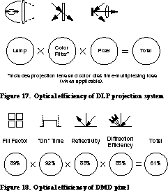
The pixel efficiency is composed of the product of the efficiencies shown in Figure 18, namely the fill factor, mirror "on" time, reflectivity, and diffraction efficiency. For the DMD pixel design used today, the pixel efficiency is 61% [44].
The color filter/projection lens efficiency depends on the dichroic filter reflection and absorption losses and reflection losses in the projection lens elements. For one-chip or two-chip DMD systems that use a rotating color disk, there is an additional loss associated with the time-multiplexing of the colors.
The lamp/reflector efficiency depends on the amount of collected light that can be used by the DMD: This is a function of the arc length of the lamp, the reflector geometry, the area of the mirror array, and the cone angle ( f/#) of the illumination and projection lens.
To understand the relationship of these parameters and their influence on the lamp/reflector efficiency, it is useful to use the concept of etendue, which is also known as "optical extent" or the "optical invariant." Etendue is a measure of the area of the light distribution, convolved with the solid angle of the light [60].
When a beam is modified by a well-corrected optical element,etendue is preserved. For example, when a well-corrected lens focuses a collimated beam to a spot, the area of the beam is reduced, but the divergence angle of the beam increases and etendue is preserved. The lamp/reflector combination has an etendue. The DMD/projection lens combination also has an etendue. If the etendue of the DMD/projection lens is smaller than that of the lamp/reflector, then the system is said to be etendue-limited. In this case, not all of the collected light from the lamp/reflector can be used by the DMD/projection lens. This is the case for all lamps but those with the shortest arc lengths.
To maximize the lamp reflector efficiency, it is necessary to minimize the etendue of the lamp in relation to that of the DMD/projection lens. The etendue of the DMD/projection lens is given by E = pi A/4f 2 , where A is the area of the DMD and f is the f /# of the projection lens. The f /# of the projection lens for the DMD is determined by the mirror rotation angle of plus/minus 10 degrees. To adequately separate the on-state light from the diffracted light produced by the mirror edges and substrate and to maximize contrast ratio, an f /# no smaller than f /2.8 is required. To preserve adequate contrast ratio in the resulting projected image, the DMD projection lens is typically fixed at f /3.0. Thus the DMD/projection lens etendue is determined solely by the area (resolution) of the DMD and increases with resolution.
For a given resolution DMD, the lamp/reflector efficiency increases as the lamp arc length (and etendue) decreases. For this reason, short arc length lamps (<2 mm) are chosen for DLP applications. For a given lamp etendue, the lamp/reflector efficiency increases as the resolution (and etendue) of the dmd increases. This latter relationship is shown graphically in Figure 19, where the modeled optical efficiency (lumens/watt) of DLP three-chip projectors is shown plotted versus DMD resolution for lamps of various powers. The SVGA resolution optical efficiencies (for the 500- and 900-watt lamps) are actual measurements from prototype projectors. Also shown is the total luminous flux in lumens that can be delivered at SVGA resolution.
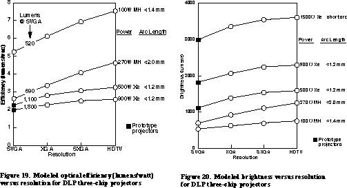
For lower lamp power (lower brightness applications), the highest optical efficiencies are achieved with metal halide(MH) lamps because of their high luminous efficacy. However, as the lamp power is increased, the arc length of metalhalide lamps must grow more rapidly than that of xenon (Xe)lamps to preserve lamp lifetime (typically determined by the time for the brightness to diminish to 50% of the stabilized brightness of a new lamp). Therefore, in DLP applications (for power levels above ~300 watts), xenon lamps, because of their shorter arc, provide better lamp/reflector collection efficiencies and higher overall system performance.
It should be noted that a large color gamut and good color balance (particularly for flesh tones) are important in high-brightness applications such as digital cinema. Although metalhalide lamps have a higher efficacy (lumens/watt) compared to xenon, not all of the luminous output can be used if color balance is to be preserved. Most metal halide lamps are typically characterized by having strong green (mercury) and greenish yellow (sodium) emission lines. These lines carry a significant portion of the lamp's luminous output. However,for proper color balance, these lines must be attenuated, with a resulting drop in the effective efficacy of the lamp.
Often it is difficult to compare projection system performance (in terms of optical efficiency) of systems using xenon lamps versus those that use metal halide lamps. Unless the color balance for these systems is adjusted to the same specification (e.g., SMPTE-C RGB points and a D65 luminant color balance), the luminous output of metal halide systems will naturally be overstated. Therefore, the lamps of Figures 19and 20 have been color-balanced to achieve a valid comparison of their performance.
In Figure 20, the modeled brightness (lumens) of DLP three-chip projectors is plotted versus DMD resolution for lamps of various powers. For the 500-, 900-, and 1,500-watt lamps,the SVGA resolution brightness levels are actual measurements from prototype projectors. Brightness levels up to 3000 lumens at SVGA resolution have been demonstrated with short arc xenon lamps. The modeled performance at HDTV resolutions with current lamps is projected to be 3600 lumens.With further improvements in short-arc xenon lamp technology, Digital Projection Ltd. (formerly Rank-Brimar) anticipates that brightness levels in excess of 10,000 lumens will be achieved in DLP brand products as resolution and format approach HDTV standards.
4.3 Maximum brightness
At high luminous flux densities (lumens/cm 2 ), optical absorption creates heating effects. Excessive temperature can cause degradation of performance for both LCDs and DMDs. in the case of LCDs, excessive heating causes degradation of the polarizers. Furthermore, without adequate cooling of the LCD panel, the temperature of the LCD material can rise above its clearing temperature T c. This renders the LCD material useless for polarization rotation and the display fails. For transmissive AM-LCD panels, a heat sink cannot be attached to the substrate, so forced air cooling must be relied upon. Larger transmissive panels mitigate this problem. Currently,AM-LCD projectors having 3000-lumen outputs use 5.8 x 5.8 in. panels.
Excessive temperatures can also affect the long-term reliability of the DMD by accelerating hinge deformation (metal creep) that can occur under high-duty-factor operation of the mirror. Special hinge alloys have been developed to minimize this deformation and guarantee reliable operation [52].High duty factors occur when the mirror is operated in one direction for a much greater part of the time, on average, than in the other direction. For example, 95/5 duty factor operation means that a mirror is 95% of the time at one rotation angle (e.g., -10 degrees) and 5% of the time at the other rotation angle (e.g., +10 degrees). This situation would correspond to DMD operation with a video source having a temporal average brightness of 5% (or 95%) of the peak brightness. Although these extreme temporal averages are unlikely to occur for extended periods of time, 95/5 duty factor is chosen as a worst case reliability test condition for hinge deformation. With current hinge metal alloys, long-term, reliable DMD operation at the 95/5 duty factor is assured,provided the operating temperature of the hinge is limited to <65 0 C.
For high-brightness applications, the mirrors can absorb enough energy to raise the hinge temperature above 65_Cunless active cooling is applied to the package. Because the dmd is reflective and built on a single-crystal silicon (X-silicon) back plane, the absorbed heat can be efficiently extracted by connecting a thermoelectric cooler (TEC) to the backside of the DMD package. In Figure 15, one of the DMD package assemblies with the thermoelectric cooler is visible. The DMD package contains "thermal vi" to provide a low-thermal-impedance path between the DMD chip and the TEC. A thermal model predicts that for a three-chip SXGA projector producing 10,000 screen lumens, the hinge temperature can be held to <65 0 C (with TEC cooling and an internal ambient air temperature of 55 0 C) .
4.4 Contrast ratio
The inherent contrast ratio of the DMD is determined by measuring the ratio of the light flux with all pixels turned on versus the flux with all pixels turned off. The system contrast ratio is determined by measuring the light flux ratio between bright and dark portions of a 4 x 4 checkerboard image according to ANSI specifications. The checkerboard measurement takes into account light scatter and reflections in the lens, which can degrade the inherent contrast ratio of the DMD.
The full on/off contrast ratio determines the dark level for scenes having a low average luminance level (e.g., outdoor night scenes) as well as the video black level. The checker-board contrast ratio is a measure of the contrast for objects in scenes containing a full range of luminance levels.
The inherent contrast ratio of the DMD is limited by light diffraction from
the mirror edges, from the underlying substrate,and from the mirror via (the
metallized hole in the middle of the mirror that acts as the mirror support
post, as shown in Figure 4). Recent architectural improvements to the
DMD pixels have led to improved contrast ratios (Table 2) [61].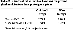 Further improvements are expected.
4.5 Accuracy and stability
Current high-brightness projection displays for use in the audio/visual rental and staging business and for private and corporate use have a number of limitations. These include warm-up or stabilization time; setup time for convergence,color balance, and gamma; and, finally, the stability of the image quality once the system is operating. Maintaining stability over a wide range of environmental conditions encountered in outdoor applications is particularly difficult.For video wall applications or other applications requiring multiple side-by-side projectors, the setup time to make all of the displays look identical is often unacceptable. Even when great care has been taken in this procedure, lack of stability makes periodic adjustments necessary.
DLP-based projection systems offer the potential of short setup time and stable, adjustment-free images. Initial stabilization time is minimal. Convergence is fixed by internal alignment of the three DMDs and is stable with time and independent of throw distance. Color balance, uniformity, and gamma are digitally controlled by pulsewidth modulation and are not affected by temperature. Brightness roll off is stable (fixed by a light integrator) and can be made small to accommodate video wall applications.
5.0 DLP BRAND PRODUCTS
Texas Instruments is teamed with numerous projection display manufacturers spanning the business (conference room), consumer (home theater), and professional (high-brightness) markets [62]. DLP brand products and prototypes serving all three market segments have been demonstrated at numerous trade shows including Cedia, Comdex, CES, Infocomm, EID,IFA, JES, Photokina, Photonics West, SID, and Satis. Shipments of the first DLP brand business projectors began in March 1996. Soon the first consumer and professional products will be available on the market.
Currently, Digital Projection Ltd., Electrohome, and Sony are developing high-brightness DLP brand products with SVGA resolution and brightness levels ranging from 1100 lumens to 3000 lumens. Announcements of the first DLP brand professional products is expected in the first quarter of 1997.
6.0 SUMMARY
DLP brand projection displays are well-suited to high-brightness and high-resolution applications. The digital light switch is reflective and has a high fill factor that results in high optical efficiency at the pixel level and low pixelation effects in the projected image. The DMD family of chips uses a common pixel design and a monolithic CMOS-like process. These factors, taken together, mean that scaling to higher resolutions is straightforward, without loss of pixel optical efficiency. At higher resolutions, the DLP brand projector becomes even more efficient in its use of light because of higher lamp-coupling efficiency. Because the DMD is a reflective technology,the DMD chip can be effectively cooled through the chip substrate,thus facilitating the use of high-power projection lamps without thermal degradation of the DMD.
DLP brand systems are all-digital (digital video in, digital light out) that give accurate, stable reproduction of the original source material. DLP brand projectors for the business (conference room) application are currently on the market. Soon, the first consumer(home theater) products will be available. DLP brand projection system prototypes for professional (high-brightness) applications have been demonstrated at up to 3000-lumen brightness for SVGA resolution. Soon, high-brightness SVGA products will be on the market, followed by XGA and SXGA products. With anticipated improvements in short-arc xenon lamp technology, it is expected that brightness levels in excess of 10,000 lumens should be achievable in DLP brand products of the future, as resolution and format approach HDTV standards.
7.0 ACKNOWLEDGEMENTS
The author wishes to acknowledge the numerous contributions of the Texas Instruments Digital Imaging staff, with special thanks to the following individuals for their many helpful suggestions during the preparation of this manuscript:Scott Dewald, Mike Douglass, Jim Florence, Richard Gale, Richard Knipe, Vishal Markandey, Greg Pettitt, Frank Poradish, and Peter van Kessel.
Special thanks also go to the editors, Sara Kay Powers and Carolyn Banks; Larry Norton, the illustrator; and the capable staff of CR&D Publishing Services.
8.0 REFERENCES
[1] E. Baumann, "The Fischer Large-Screen Projection System," J.
SMPTE, Vol. 60, pp. 344-356 (April 1953). Copyright 1997, Texas Instruments, All Rights Reserved
[2] R.J. Gove, "DMD Display Systems: The Impact of an All-Digital Display," Society
for Information Display Inter-national Symposium (June 1994).
[3] L.J. Hornbeck and W.E. Nelson, "Bistable Deform-able Mirror Device," OSA
Technical Digest Series, Vol. 8, Spatial Light Modulators and Applications,
p. 107 (1988).
[4] W.E. Nelson and L.J. Hornbeck, "Micromechanical Spatial Light Modulator
for Electrophotographic Printers," SPSE Fourth International Congress on
Advances in Non-Impact Printing Technologies, p. 427 (March 20, 1988).
[5] L.J. Hornbeck, "Deformable-Mirror Spatial Light Modulators (Invited Paper)," Spatial
Light Modulators and Applications III, SPIE Critical Reviews, Vol. 1150,
pp. 86- 102 (August 1989).
[6] T.J. Sheerer, W.E. Nelson, and L.J. Hornbeck, "FEM Analysis of a DMD," Seventeenth
Nastram User Colloquium, NASA Conf. Pub. 3029, p. 290 (1989).
[7] J.B. Sampsell, "An Overview of Texas Instruments Digital Micromirror Device
(DMD) and Its Application to Projection Displays," Society for Information
Display Internatl. Symposium Digest of Tech. Papers, Vol. 24, pp. 1012-1015
(May 1993).
[8] L.J. Hornbeck, "Current Status of the Digital Micromirror Device (DMD) for
Projection Television Appli-cations (Invited Paper)," International Electron
Devices Technical Digest, pp. 381-384 (1993).
[9] J.M. Younse and D.W. Monk, "The Digital Micromirror Device (DMD) and Its
Transition to HDTV," Proc. of 13th International Display Research Conf. (Late
News Papers), pp. 613-616 (August 31-September 3, 1993).
[10] J.B. Sampsell, "The Digital Micromirror Device," 7th ICSS&A, Yokohama,
Japan (1993).
[11] J.M. Younse, "Mirrors on a Chip," IEEE Spectrum, pp. 27-31 (November
1993).
[12] J.M. Younse, "DMD Projection Display Technology (Invited Talk)," IEEE
Multimedia Symposium, Richardson, TX (April 19, 1994).
[13] M.A. Mignardi, "Digital Micromirror Array for Pro-jection TV," Solid
State Technology, Vol. 37, pp. 63-66 (July 1994).
[14] K. Ohara and R.J. Gove, "DMD Display and Its Video Signal Processing,"
The Institute of Television Engineers Ja-pan 1994 Annual Convention, ITEC ?94,
Saga, Japan (July 1994).
[15] V. Markandey, T. Clatanoff, R. Gove, K. Ohara, "Mo-tion Adaptive Deinterlacer
for DMD (Digital Micromirror Device) Based Digital Television," IEEE Trans.
on Consumer Electronics, Vol. 40, No. 3, pp. 735-742 (August 1994).
[16] J.M. Younse, "Commercialization of Digital Micromirror Display Technology," Conference
for Commer-cialization of Microsystems, Banff, Alberta, Canada (September
13, 1994).
[17] D. Monk and R. Gale, "The Digital Micromirror De-vice for Projection Display
(Invited Paper)," Microelectronic Engineering, Vol. 27, pp 489-493 (1995).
[18] V. Markandey and R. Gove, "Digital Display Sys-tems Based on the Digital
Micromirror Device," SMPTE 136th Technical Conference and World Media Expo
(Octo-ber 1994).
[19] D.W. Monk, "Digital Micromirror Device Technol-ogy for Projection Displays,"
EID Exhibition & Conference, Sandown, UK (October 26, 1994).
[20] R.J. Gove, V. Markandey, S. Marshall, D. Doherty, G. Sextro, and M.
DuVal, "High Definition Display System Based on Digital Micromirror Device," International
Work-shop on HDTV (HDTV?94), International Institute for Communications,
Turin, Italy (October 1994).
[21] J.B. Sampsell, "An Overview of the Performance13 Envelope of Digital Micromirror
Device Based Projection Dis-play Systems," SID 94 Digest, pp. 669-672 (1994).
[22] C. Tew, L. Hornbeck, J. Lin, E. Chiu, K. Kornher, J. Conner, K. Komatsuzaki,
and P. Urbanus, "Electronic Con-trol of a Digital Micromirror Device for Projection
Displays (Invited Paper)," IEEE International Solid-State Circuits Di-gest
of Technical Papers, Vol. 37, pp. 130-131 (1994).
[23] G.A. Feather and D.W. Monk, "The Digital Micromirror Device for Projection
Display," IEEE Interna-tional Conference on Wafer Scale Integration, San
Francisco, CA (January 18-20, 1995).
[24] W.E. Nelson and R.L. Bhuva, "Digital Micromirror Device Imaging Bar for
Hardcopy," Color Hardcopy and Graphic Arts IV, SPIE, Vol. 2413, San Jose,
CA (February 1995).
[25] E. Chiu, C. Tran, T. Honzawa, and S. Namaga, "De-sign and Implementation
of a 525 mm 2 CMOS Digital Micromirror Device (DMD) Chip," Proc. 1995 International
Symposium of VLSI Technology Conf., p. 127, Taipei, Taiwan (1995).
[26] B.R. Critchley, P.W. Blaxtan, B. Eckersley, R.O. Gale, and M. Burton, "Picture
Quality in Large-Screen Projectors Using the Digital Micromirror Device," SID
95 Digest, pp. 524-527 (1995).
[27] G. Sextro, T. Ballew, and J. Iwai, "High-Definition Projection System Using
DMD Display Technology," SID 95 Digest, pp. 70-73 (1995).
[28] M.R. Douglass and D.M. Kozuch, "DMD Reliability Assessment for Large-Area
Displays," Society for Informa-tion Display International Symposium Digest
of Technical Papers, Vol. 26 (Applications Session A3), pp. 49-52 (May 23-25,
1995).
[29] G. Feather, "Digital Light Processing?: Projection Display Advantages of
the Digital Micromirror Device?," 19th Montreux Television Symposium (June
1995).
[30] J.M. Younse, "DMD Microelectromechanical (MEMS) Technology (Keynote Address)," Society
of Experi-mental Mechanics (SEM) UACEM Conference, Worcester, MA, (July 6,
1995).
[31] J.M. Younse, "DMD Display Technology (Invited Talk)," Naval Research
Center, Washington, DC (September 5, 1995).
[32] G. Hewlett and W. Werner, "Analysis of Electronic Cinema Projection With
the Texas Instruments Digital Micromirror Device? Display System," 137th
SMPTE Tech-nical Conference, Los Angeles, CA (September 6-9, 1995).
[33] J.M. Younse, "DMD Display Technology (Invited Talk)," U.S. Government?s
Large Display Working Group Meeting, NUWC, Newport, RI (September 21, 1995).
[34] T. Hogan, J. Hortaleza, "Low Temperature Gold Ball Bonding for Micromechanical
Device Interconnections," Ul-trasonic Industry Association, Columbus, OH
(October 18, 1995).
[35] J.M. Younse, "Projection Display Systems Based on the Digital Micromirror
Device (DMD)," SPIE Conference on Microelectronic Structures and Microelectromechanical
Devices for Optical Processing and Multimedia Applications, Austin, TX, SPIE
Proceedings, Vol. 2641, pp. 64-75 (Octo-ber 24, 1995).
[36] L.J. Hornbeck, "Digital Light Processing and MEMS: Timely Convergence for
a Bright Future (Invited Plenary Pa-per)," Proc. SPIE, Vol. 2639, Micromachining
and Microfabrication Process Technology, p. 2 (1995)?Abstract Only. Color
reprint of complete paper available. Call 1-888- DLP-BYTI (1-888-357-2984).
[37] W.E. Nelson, "Tutorial on Optical Printheads," IS&T Eleventh International
Congress on Advances in Non-Impact Printing Technologies, Hilton Head, SC
(October
29, 1995).
[38] L. Yoder, "The Fundamentals of Using the Digital Micromirror Device (DMD)
for Projection Displays," Proc. International Conference on Integrated Micro/
Nanotechnology for Space Applications, sponsored by NASA and Aerospace Corp.,
Houston, TX (October 30-November 3, 1995).
[39] J. Iwai, G. Sextro, "High-Definition Projection Sys-tem Using DMD Technology," IEEE
1995 International Workshop on HDTV and the Evolution of Television, Taipei,
Taiwan (November 15-17, 1995).
[40] G. Deffner, "Eye Movement Recordings to Study Determinants of Image Quality
in New Display Technology," Eye Movement Research, pp. 479-490, J.M. Findlay,
R. Walker, and R.W. Kentridge (eds.), Elsevier, Amsterdam (1995).
[41] D. Fritsche, V. Liu, V. Markandey, and S. Heimbuch, "Integration of Today?s
Digital State With Tomorrow?s Vi-sual Environment," Proc. SPIE, Vol. 2650,
Projection Displays II, pp. 9-17 (1996).
[42] V. Markandey, T. Clatanoff, and G. Pettitt, "Video Processing for DLP Display
Systems," SPIE Photonics West ?96, San Jose, CA (January 27-February 2, 1996).
[43] R. Howell and M. Mignardi, "Fabrication of the Digi-tal Micromirror Device
(Invited Paper)," SID Displaywork 1996, Manufacturing Technology Conference
(February 7, 1996).
[44] J. Florence and L. Yoder, "Display System Architec-tures for Digital Micromirror
Device (DMD) Based Projectors," Proc. SPIE, Vol. 2650, Projection Displays
II, pp. 193-208 (1996).
[45] V. Markandey, G. Hewlett, and G. Pettitt, "Digital Light Processing: The
Convergence of Television and Com-puter Display," 30th SMPTE Advanced Technical
Conference 1996 Proceedings, pp. 150-160 (1996).
[46] D. Monk, "Digital Light Processing With the Digital Micromirror Device,"
Electronic Displays ?96, Chemnitz, Ger-many (April 24-25, 1996).
[47] G. Pettitt, A. DeLong, and A. Harriman, "Colorimet-ric Performance Analysis
for a Sequential Color DLP Projection System," SID ?96, San Diego, CA (May
1996).14
[48] R.G. Fielding, M. Burton, and T. Bartlett, "Colorim-etry Performance of
a High Brightness DMD Based Optical System," SID ?96, San Diego, CA (May
1996).
[49] M.R. Douglass and C. Malemes, "Reliability of Dis-plays Using Digital Light
Processing," SID ?96, San Diego, CA (May 1996).
[50] L.J. Hornbeck, "Digital Light Processing: A New MEMS-Based Display Technology
(Keynote Address), "Tech-nical Digest of the IEEJ 14th Sensor Symposium,
pp. 297-304, Kawasaki, Japan (June 4-5, 1996).
[51] L.J. Hornbeck, "Digital Light Processing and MEMS, Reflecting the Digital
Display Needs of the Networked Soci-ety (Invited Plenary Paper)," SPIE Europto
Proceedings, Vol. 2783, pp. 2-13 Besancon, France (June 12-13, 1996).
[52] R.L. Knipe, "Challenges of a Digital Micromirror Device: Modeling and Design," SPIE
Europto Proceedings, Vol. 2783, pp. 135-145 (June 12-13, 1996).
[53] V. Markandey and G. Hewlett, "Digital Light Pro-cessing: A DSP Powered
Multimedia Display," DSP & Multimedia Technology, Vol. 5, No. 4 (July/August
1996).
[54] L.J. Hornbeck, "Digital Light Processing and MEMS: An Overview (Invited
Paper)," Digest of IEEE/LEOS 1996 Summer Topical Meetings, Optical MEMS and
Their Appli-cations, WA3, pp. 7-8, Keystone, CO (August 5-9, 1996).
[55] F. Skaggs, "Automatic Testing of the Digital Micromirror Device (DMD)," Digest
of IEEE/LEOS 1996 Summer Topical Meetings, Optical MEMS and Their Appli-cations,
WB2, pp. 11-12, Keystone, CO (August 5-9, 1996).
[56] W.E. Nelson, "Digital Light Processing for Color Printing (Invited Paper)," Digest
of IEEE/LEOS 1996 Sum-mer Topical Meetings, Optical MEMS and Their Applications,
WC3, pp. 19-20, Keystone, CO (August 5-9, 1996).
[57] M. Mignardi, R. Howell, "The Fabrication of the Digi-tal Micromirror Device,"
EF/SEMI Conference, Commercialization of Microsystems ?96, Kona, HI (October
6-11, 1996). Proceedings in progress.
[58] L.J. Hornbeck, "Digital Light Processing for Projec-tion Displays: A Progress
Report (Invited Paper)" SID EuroDisplay ?96, Proceedings of the 16th International
Dis-play Research Conference, pp. 67-71, Birmingham, England (October 14-18,
1996).
[59] L.J. Hornbeck, "DLP (Digital Light Processing) fur ein Display mit Mikrospiegel-Ablenkung," Fernseh-und
Kino-Technik, pp. 555-564, Berlin, Germany (October 1996) ? In Color.
[60] M.S. Brennesholtz, "Light Collection Efficiency for Light Valve Projection
Systems," Proc. SPIE, Vol. 2650, Pro-jection Displays II, pp. 71-79 (1996).
[61] J. Florence, R. Miller, and T. Bartlett, "Contrast Ra-tio in DMD-Based
Projection Systems," to be presented at SID ?97, Boston, MA (May 1997).
[62] Digital Light Processing World Wide Web site: http:// www.ti.com/dlp15
21st, The VXM Network, https://vxm.com